Printed electronics laboratory
Facilities adapted to the needs of paper electronics
- Print substrates with functional (conductive, resistive, dielectric, electroluminescent, etc.) inks or barrier inks
- Print RFID antennas using conventional printing facilities
- Create electroluminescent surfaces
General informations
Printed electronics is becoming a way for paper & board manufacturers, printers and converters to diversify. These new printing and functionalisation techniques are opening the doors to new high value-added markets where there is little competition with respect to paper and board.
As a result of its development projects and investments made in this field (e.g. the EIPIT* project) the CTP now possesses an advanced printed electronics laboratory.
The CTP is able to test all types of printing substrate (cellulose, plastic, textiles) with all processes that can be used in the field of printed electronics.
*EIPIT –French acronym meaning Printed Electronics for Printers and Converters


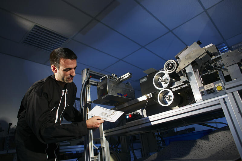
i-SpeedFlex
Context
The CTP's printed electronics laboratory is capable of producing functional systems based on different printing facilities.
Since 2008, the CTP has been developing its own laboratory facilities in addition to the conventional equipment.
These "made in CTP" facilities are used to develop prototypes and printed samples that meet our client's own specifications.
The CTP's laboratory thus operates several specific, unique pilots dedicated to printed electronics.

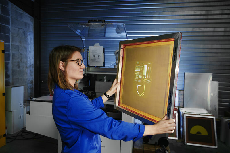
Screen for ScreenInk
Equipments
- Flexographic: i-Speed-Flex
- Inkjet: high-speed inkjet print head (i-SpeedJet), functional ink printing unit (JEEP)
- Abrasion testing and laser cutting
- Screen printing: ScreenInk
- Printed electronics assembly: customised Scara robot: PAPRIKA

Illuminate paper-board
Studies
All types of study are possible. They are defined in accordance with the expertise required prior to carrying out the work.